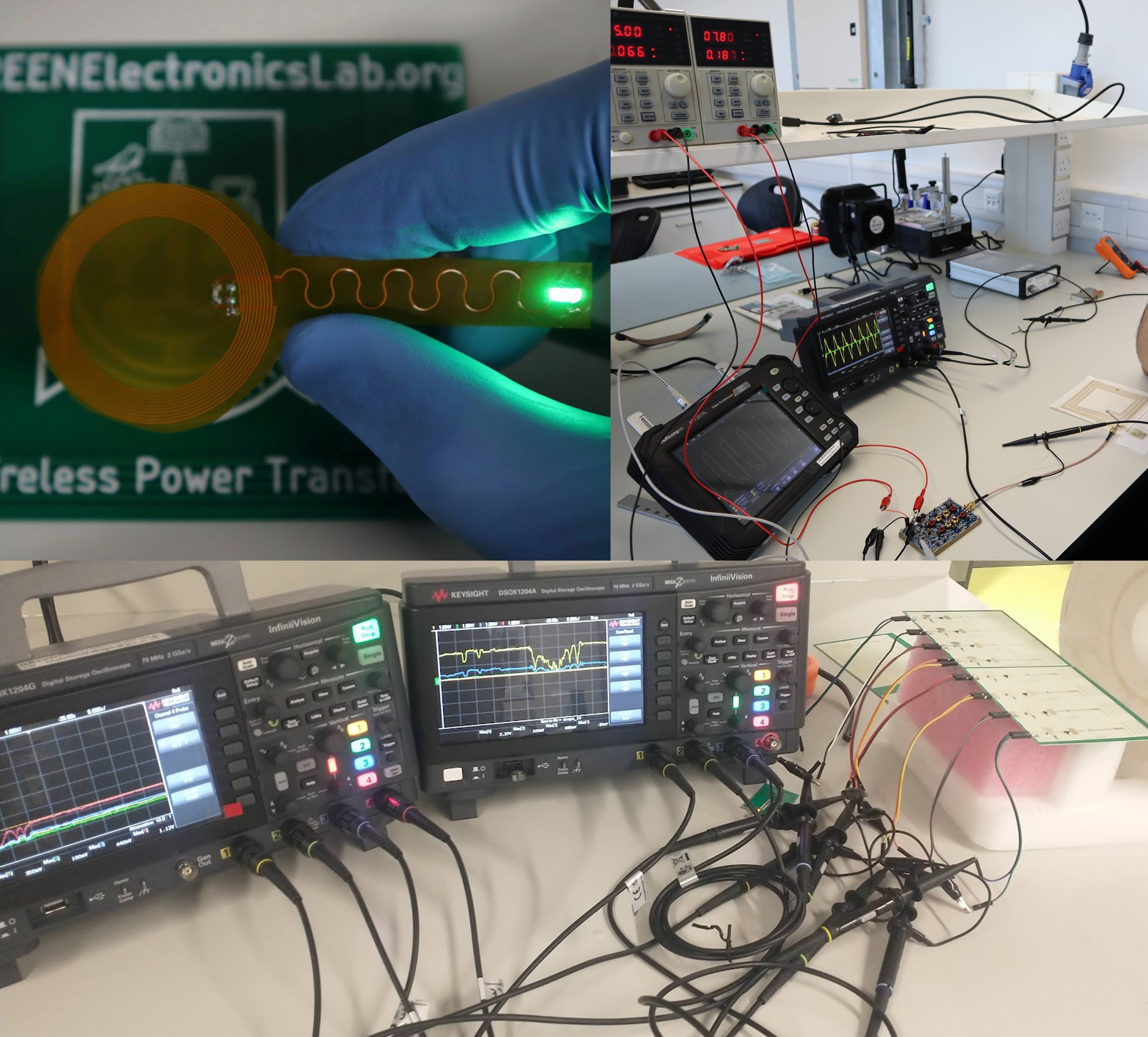
We have extensive and world-leading facilities for large-area electronics manufacturing, RF and microwave characterisation, and electronics integration towards complete functional systems.

RF, Microwave, and Wireless

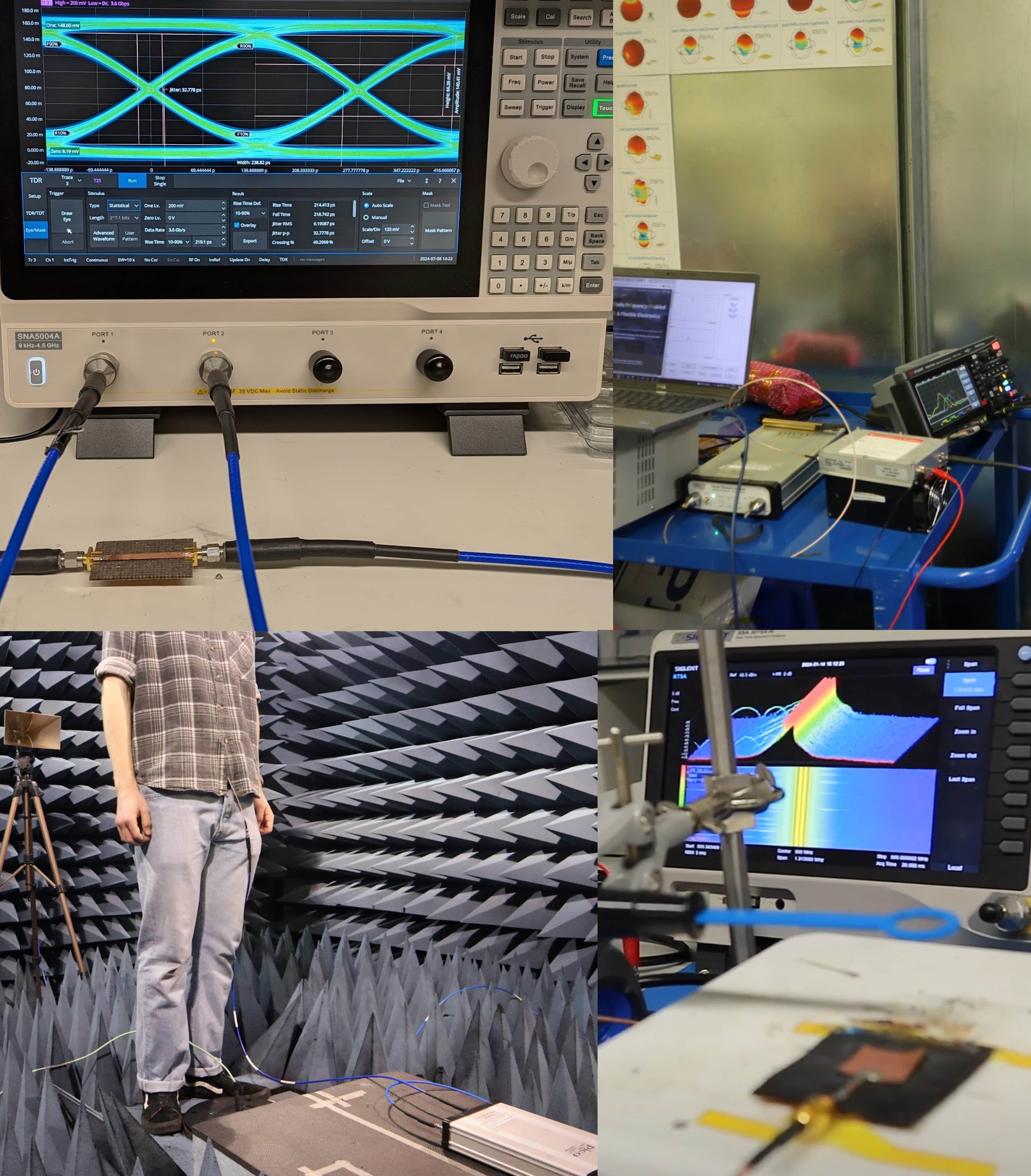
We have dedicated and automated equipment for in-situ RF measurements, including unconventional devices/sensors (refer to the shared equipment section for mmWave/THz facilities).

• Multiple Vector Network Analyzers (VNAs) including 2-port (300 kHz to 6/7.5 GHz) and 4-port systems (9 kHz to 4.5 GHz), and compact/portable VNAs for in-situ sensor and antenna measurements
• Real-time spectrum analysis up to 7.5 GHz (40 MHz RT bandwidth).
• Time-domain reflectometry (TDR), eye diagrams and signal integrity measurements (4.5 GHz/>GBPS).
• Multiple dual-ridge horn antennas 0.7-8+ GHz, and other CP/LP reference antennas.
• UHF RFID readers, providing RSSI and phase data in the US/EU bands.
• 15+ portable NanoVNAs for paralellized testing of sensors (100 kHz to 500 MHz).
• Material characterization (permittivity and loss-tangent) from under 1 MHz to 1+ GHz.
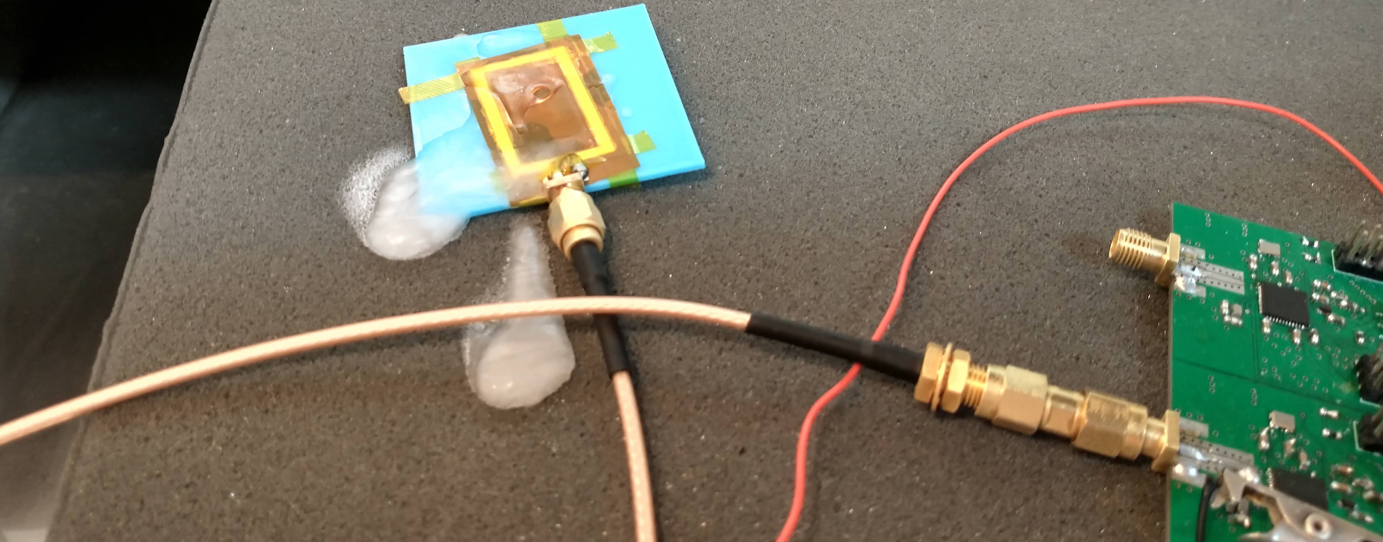
DC, Low-Power, and Mixed-Signal

Complementing our work on energy harvesting and IoT systems, we have extensive capabilities for characterizing low-power embedded systems, and bespoke analogue/mixed-signal electronics for sensing, energy harvesting, and computing.

• Multiple digital oscilloscopes with >50 MPTs records over 4+ channels.
• Portable instrumentation for field measurements and embedded systems testing.
• Extensive development boards covering most popular Arm-based MCUs and wireless SoCs (TI, NXP, ST, nRF, Arduino etc).

Printed, 3D, E-Textile, and Large-Area Electronics

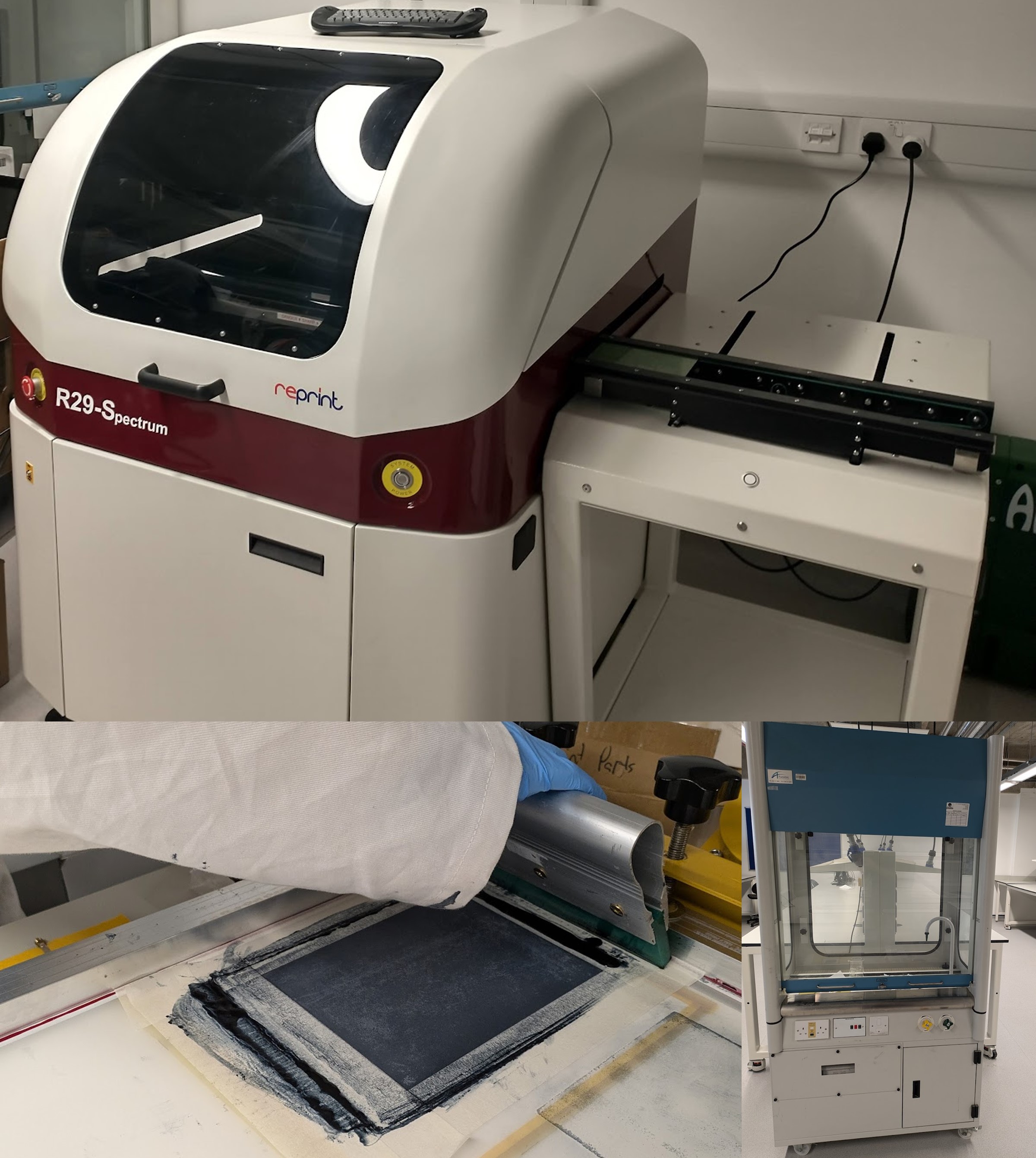
Funded by the UK Royal Society, we have developed a bespoke system for automated screen and stencil printing of thick-film circuits using non-metal functional inks, as well as extensive processing capabilities for 3D-printed and moulded circuits.

• Screen printing of organic polymers/MOS/carbon-based inks (manual and automated).
• E-textile fabrication including embroidery, printing, and heat-pressing.
• Functional sensing and RF composite formulation and moulding based on metal/non-metal fillers.
• Printed liquid metal components and channels, for wireless and microwave devices.

Shared Infrastructure: CAE, ANALOGUE, and JWNC

We have full access to two internationally-leading EPSRC Strategic Equipment Suites, through the CAE, we have:
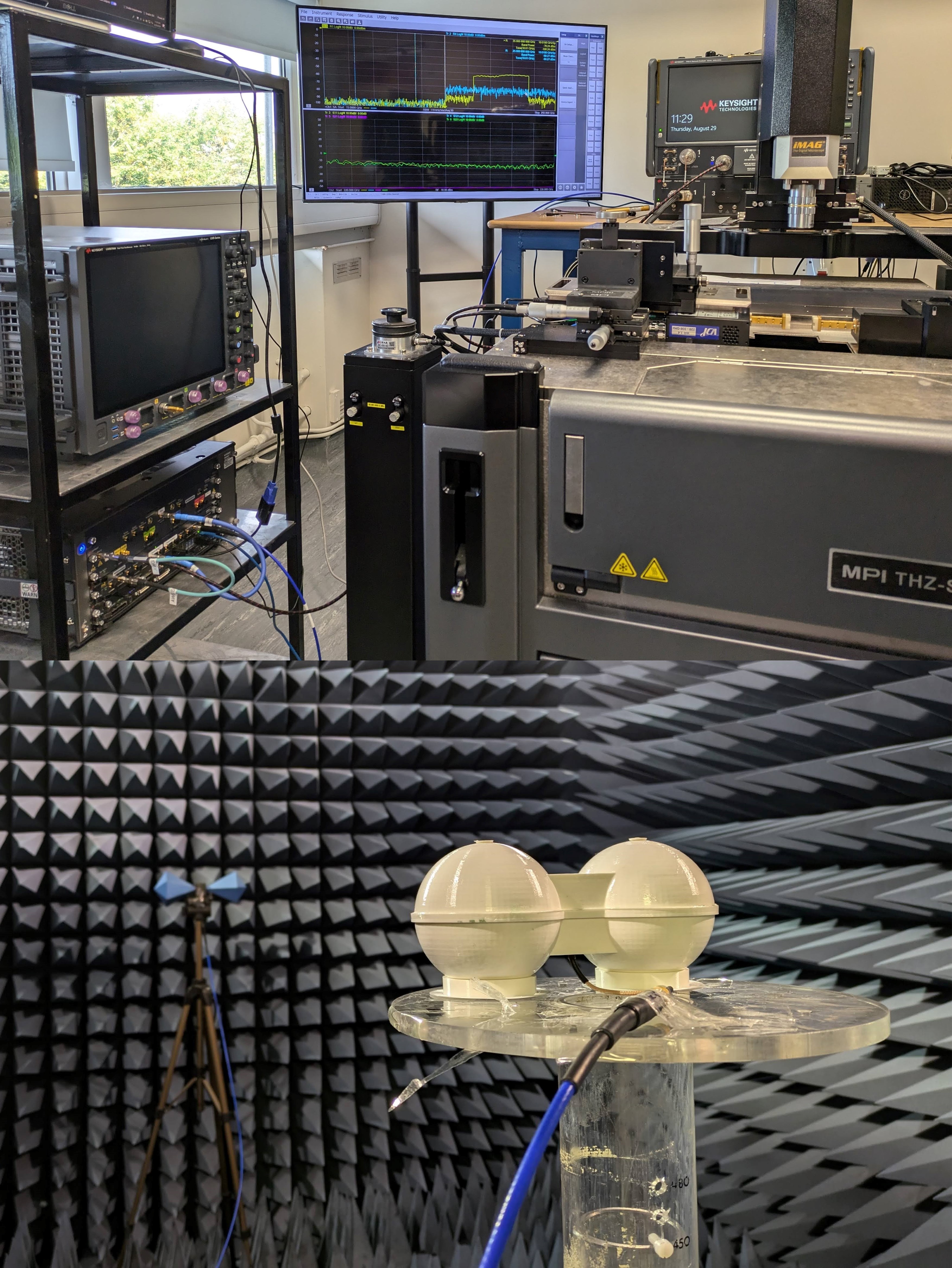
• Full Anechoic Chamber usable for antenna measurements up to 20 GHz, including 2D patterns and direct gain measurements (comparison/two-antenna methods).
• Extensive Vector Network Analysis for waveguide and on-wafer measurements, from 10 MHz to 1,100 GHz (covering the full mmWave bands, in banded waveguides), and full on-wafer capabilities up to 330 GHz.
• RF noise measurements (up to 50 GHz) and impedance tuners/load-pull.
• Full device characterisation up to 3 kV, including CV/IV measurements.

In additive manufacturing and semiconductor integration/packaging, through ANALOGUE Suite, we have:
• Extensive micron-scale 2D and 3D printing, for high-resolution printed electronics.

For nano-fabrication and characterisation, we also leverage the James Watt Nanofabrication Centre (JWNC) including SEMs, XRD, AFM microscopy, and extensive lithography/deposition capabilities.

Phone

(+44) 0141 330 3601

Address

James Watt South, School of Engineering
Univeristy of Glasgow
Glasgow, G12 8QQ
University of Glasgow